Physics & modeling
Interactions between light and matter, thermal transport, and free space propagation.
Lumerical · COMSOL · rigorous coupled wave analysis · ZemaxFrom programmable photonics to intelligent photonic matter
I develop nonvolatile silicon photonic devices and systems, combining heterogeneous material integration with foundry scale engineering, optical computing, and practical deployment.
Platform focus
Full spectrum capability
I move fluently between fundamental physics and practical engineering, turning an optical concept into a fabricated, controlled, packaged, and measured system.
Interactions between light and matter, thermal transport, and free space propagation.
Lumerical · COMSOL · rigorous coupled wave analysis · ZemaxPhotonic components, programmable meshes, meta optics, and foundry layouts.
Python · mask layout · Cadence · process design kitsCleanroom process development from start to finish, including phase change material integration.
Lithography · Deposition · EtchAutomated optical, electrical, material, and surface measurements.
LabVIEW · optical spectrum analyzer · X ray diffraction · atomic force microscopyScalable pulse control, instrument automation, signal transfer, and printed circuit board design.
Python · MATLAB · LabVIEWElectrical and photonic packaging toward robust, plug and play prototypes.
Fiber coupling · Integration · ValidationResearch impact & service
Research program
My work follows the full stack: modeling, device design, nanofabrication, automated characterization, electronics, packaging, and scalable photonic architectures.
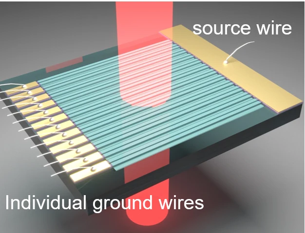
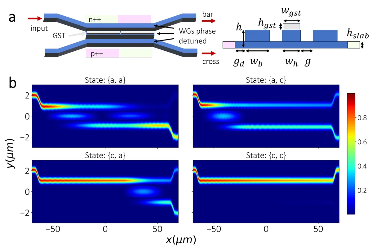
Building nonvolatile photonic gate arrays that route and process light with precise, multibit control, without the static power cost of conventional tuning.
Lead and senior author work
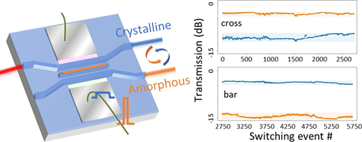
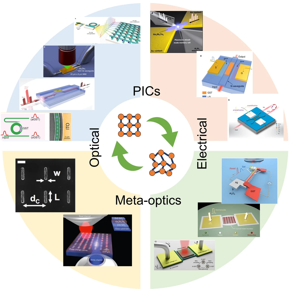
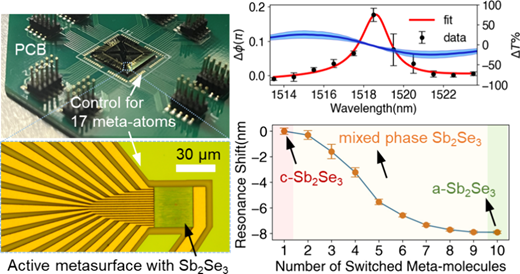
4 papersIntegrating germanium antimony telluride (GST), antimony sulfide (Sb2S3), and antimony selenide (Sb2Se3) with silicon and silicon nitride platforms, from material characterization through nanofabrication, electrical control, and system level validation.
Lead and senior author work
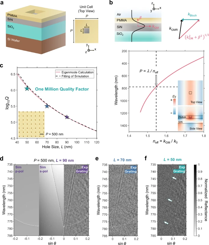
4 papersDesigning electrically addressable metasurfaces and optical resonators with high quality factors for compact wavefront control, sensing, and computation in free space.
Lead and senior author work
3 papersFuture research vision
My independent program will connect heterogeneous material platforms, photonic circuits with autonomous configuration, and packaged optical interfaces across shared infrastructure for design, fabrication, packaging, and testing.
Unify photonic hardware, control algorithms, sensing, and nonvolatile memory so optical systems can interpret their environment, retain useful states, and adapt their response.
Connect programmable photonic nodes through shared optical signals and local feedback, enabling distributed systems to learn cooperatively, coordinate behavior, and improve without centralized control.
Merge photonic integrated circuits, meta optics, heterogeneous materials, and embedded control into adaptive optical bodies that sense, compute, remember, and reshape light across guided and free space.
Latest highlight · 2026
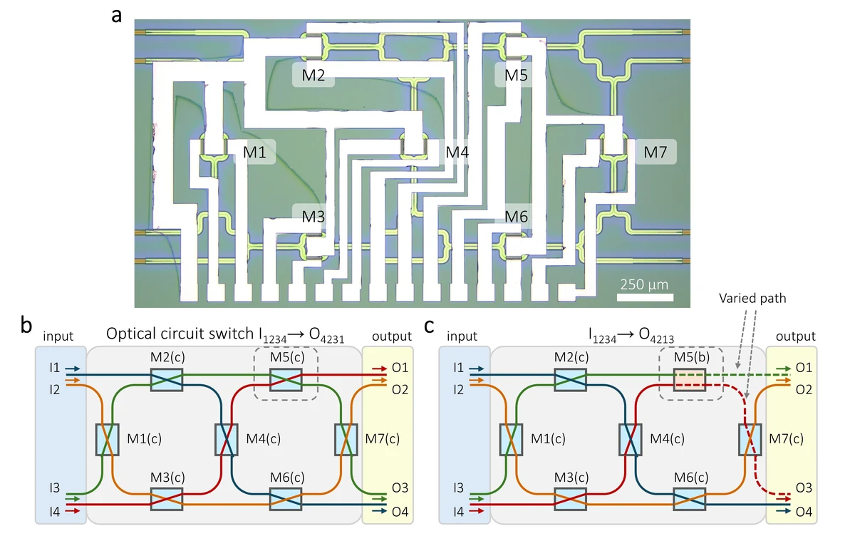
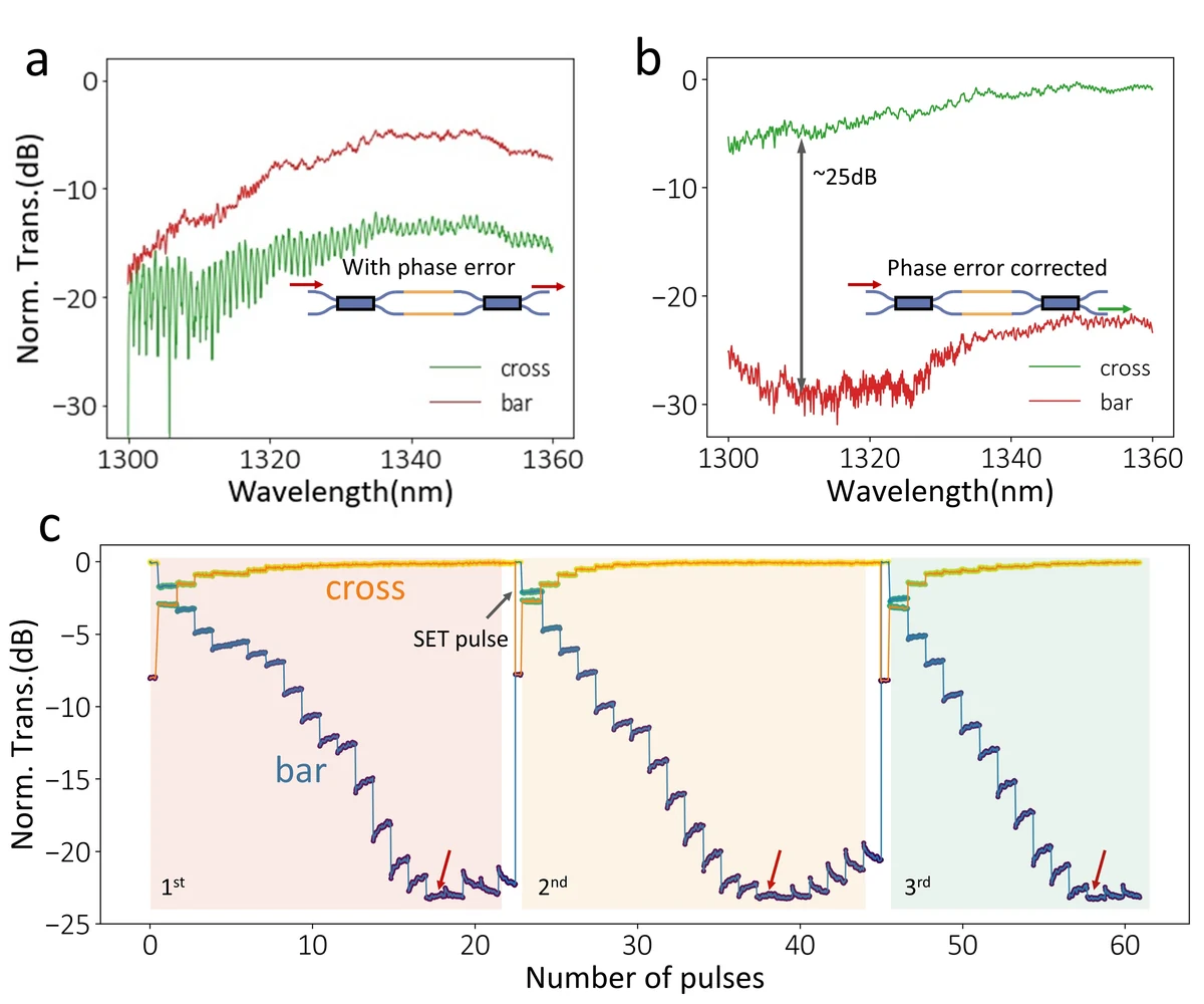
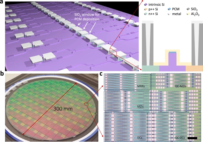
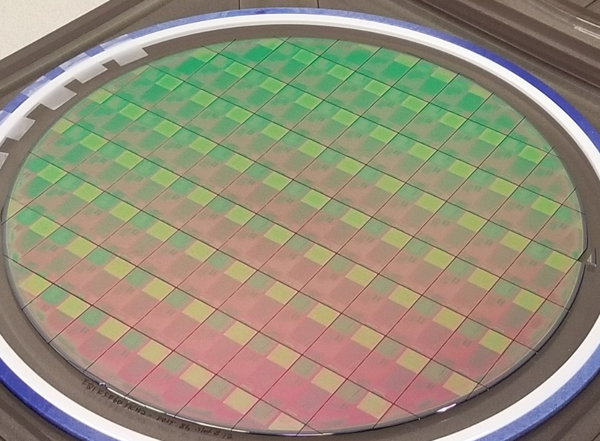
The nonvolatile electro-optical programmable gate array (NEO-PGA) brings the flexibility of programmable photonics to a scalable 300 mm silicon platform using phase change materials and a “program, then verify” feedback method.
Experience
2025 to Present
2024
2020 to 2025
2018 to 2020
Teaching philosophy
I help students connect physical intuition, mathematical models, and system level abstraction, then move confidently between theory, simulation, data, and hardware.
I have mentored more than 10 undergraduate and master's students across photonic design, fabrication, and experiments, with outcomes including coauthored journal papers and conference presentations.
Teaching experience
8 coursesFull length teaching and course assistant roles across the University of Washington and Columbia University.Designed the course with a new faculty member from the ground up, reviewing lecture notes and creating a complete set of homework assignments and laboratory instructions.
Designed and led a new hands on experiment for undergraduate and master's students, providing practical device characterization experience and connecting theory to measurement.
Next chapter
I am exploring faculty positions and advanced R&D roles where rigorous science, scalable engineering, and meaningful mentorship meet.